
The launch post ended on a claim: the manufacturing files are in the repository, so you can make one of these without me. This post is the part that comes after that sentence. It walks the actual order — the same one in the video above — from hw/v1/fab/ to a padded box of assembled boards.
None of it is hard. But a handful of choices on the quote page are the difference between a board that works and a board with a dead touch pad, and a handful of warnings look alarming and mean nothing. Those are what this post is really about.
Watch it first
The video is the primary source here: it is the click-by-click version, screen recorded, with the real quote page rather than a description of it. Everything below is the written companion — the numbers to type in, the files to reach for, and the reasoning behind the settings, in a form you can keep open in a second tab while you order.
If you only read one section, read the four options that matter.
The whole order is three files
Everything the fab needs is checked into hw/v1/fab/. You upload three of them.
| File | Where it goes |
|---|---|
openmicro-gerbers.zip | The PCB quote page — upload the zip as-is, do not unpack it |
openmicro-bom.csv | The assembly step — what to place |
openmicro-smt.csv | The assembly step — where to place it |
Two more files sit alongside them and are not part of the order. gerbers/ is the same package unzipped, there for review and diffing. openmicro-pos-all.csv is a position file for every footprint including the through-hole parts and mounting holes — it is for building fixtures and for inspection, not for the pick-and-place. Uploading it instead of openmicro-smt.csv will ask the machine to place parts that are not machine-placeable.
The BOM and the CPL come from different places, which is worth knowing when you go to regenerate them. The BOM is emitted by the CoHDL compiler from the schematic source in hw/v1/src/. The Gerbers and the CPL come from the routed board, hw/v1/pcb/openmicro.kicad_pcb, via KiCad 10. The design is the source of truth for what; the layout is the source of truth for where.
Part one: the board
Upload the Gerbers
Drop openmicro-gerbers.zip onto the quote page. It contains the four copper layers, both paste and solder-mask layers, both silkscreens, the edge cuts, and separate Excellon drill files for plated and non-plated holes.
One thing to actually look at rather than skip: the layer names in this package follow an Altium-style convention rather than KiCad's, so the inner planes arrive as Ground Layer 1.g1 and Ground Layer 2.g2 rather than *.g2l/*.g3l. JLC's parser handles this, but open the Gerber viewer after upload and confirm the assignment anyway: F.Cu signal, In1 ground plane, In2 ground plane, B.Cu signal, top to bottom. Thirty seconds there is cheap insurance against a board with its planes in the wrong order.
While you are in the viewer, the board should read as 95 × 95 mm with a square 4×4 key grid, thirteen keyswitch cutouts, and — this is the one that startles people — thirteen small rectangular openings in the board itself under the key positions. Those are supposed to be there. The key LEDs are reverse-mount and fire up through the board toward the keycaps.
The four options that matter
Most of the quote page can stay on its defaults. Four fields cannot.
| Option | Set it to |
|---|---|
| Layers | 4 |
| Impedance control / stackup | JLC04161H-7628 |
| Surface finish | ENIG |
| Thickness | 1.6 mm, 1 oz copper, FR-4 |
Four layers is not negotiable — the routing depends on two solid internal ground planes, and the file set will not make sense as a 2-layer order.
The stackup matters because of USB. The differential pair to the USB-C receptacle is routed to a target of 100 Ω differential and 50 Ω single-ended, against a dielectric of 0.2 / 1.03 / 0.2 mm. JLC04161H-7628 is the standard 4-layer stackup that matches those numbers. Pick a different stackup and the geometry that was routed for you stops meaning what it meant; the pair targets live in hw/v1/out/differential_pairs.csv if you want to check the arithmetic yourself.
ENIG is the one that silently ruins a board. TP1 is not a component — it is a nine-millimetre disc of bare copper acting as a capacitive touch electrode. On HASL it comes back as an uneven, oxidising blob of solder, and the sensor's baseline drifts with it. ENIG gives you a flat, stable, gold-over-nickel surface that a finger reads consistently. It costs a few dollars more on a prototype run. Pay it.
The one setting that will quietly cost you a board is the surface finish. The touch pad is bare copper by design — order ENIG.
Note that PCB quantity and assembly quantity are separate choices, each with its own minimum, and the fab's minimums change over time — read them off the quote page rather than assuming. Ordering the board minimum and assembling fewer of them is a perfectly reasonable way to keep a spare bare PCB around.
Part two: the assembly
This board is assembled on both sides
Turn on assembly and you are immediately asked which side to populate. The honest answer for this board is both, and it is worth knowing why before you see the price change.
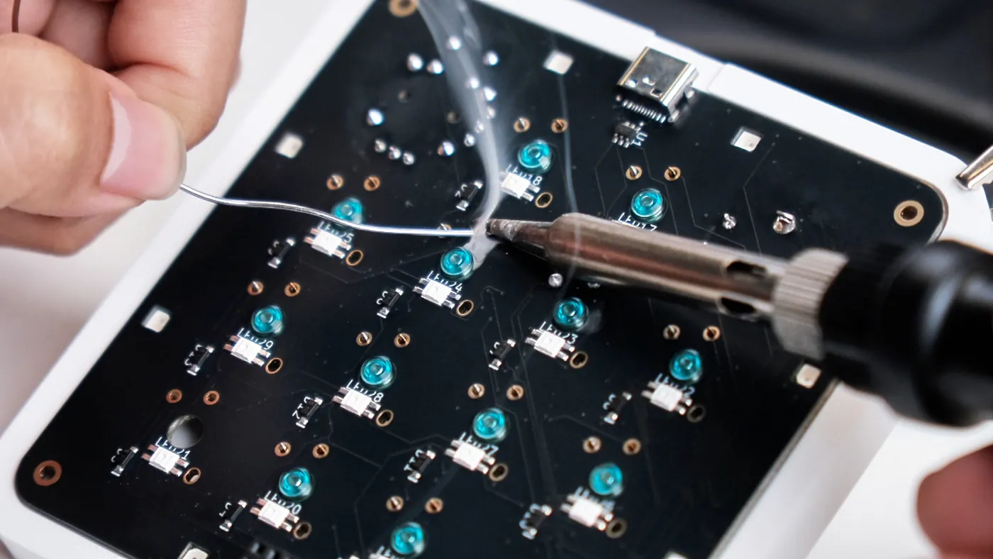
The pick-and-place file carries 68 placements. Fifty-three of them are on the bottom: the STM32, the USB-C receptacle, the ESD diode, the LDO, the crystal, all thirteen matrix diodes, the SWD socket, most of the passives, and the thirteen reverse-mount key LEDs that shine up through those board cutouts. The remaining fifteen are on the top: the eight perimeter underglow LEDs and five passives.
You can, in principle, order bottom-side assembly only and hand-solder the eight underglow LEDs yourself. They are SK6812MINI-E packages on a shared data chain, so a single bad joint takes out everything downstream of it. Unless you have a reason to, let the machine do all sixty-eight.
The BOM and the CPL
Upload openmicro-bom.csv and openmicro-smt.csv. The BOM's columns are Manufacturer,Comment,Designator,Footprint, where Comment holds the manufacturer part number — STM32F072CBT6, AP2112K-3.3TRG1, 1N4148W-7-F, and so on. That is deliberate: the MPN is what the matching step searches on, and a real part number resolves to a real catalogue entry far more reliably than a value string does.
The CPL is in millimetres, origin at the board's lower-left corner, Y-up, with rotations following KiCad's orientation convention. Its own Comment column carries friendly values — 100nF, SK6812, Diode_1N4148 — rather than MPNs. That mismatch between the two files is fine and expected: the two files are joined on the designator, not on the comment.
The five rows that are not parts
The BOM describes the design, and the design contains things that are not components. Five rows will not match anything in the catalogue, and both are supposed to fail:
TP1—COPPER-TOUCH-9MM, manufacturern/a. The touch electrode. It is copper on the board, not a thing to buy.H1–H4—MOUNT-M2-PLATED-2.2MM, manufacturern/a. Plated mounting holes.
Neither appears in the CPL, so nothing will be placed for them regardless. Mark them as do-not-place, or strip them from your copy of the BOM before uploading if you would rather not look at the warnings.
A second group will match but must not be assembled, because they are through-hole parts the fab is not populating:
SW3–SW15— thirteen low-profile keyswitchesSW1— theEC11rotary encoderJ1— theRKJXVanalog joystick
These are in the BOM for sourcing, and absent from the CPL on purpose. You buy them separately and solder them by hand once the boards arrive. The switches in particular are a keyboard-hobby part, not an electronics-distributor part — the BOM lists a low-profile 55 g switch, and any Choc V2-compatible switch in a weight you like will drop into the same footprint.
The placement preview is the real review
After matching, JLC renders every part onto a picture of your board. This is the single highest-value minute in the whole order, because it is the last point at which a rotation error is free to fix.
Rotations in the CPL follow KiCad's convention; assembly houses then apply their own per-part corrections for how a component sits in its tape. Usually this is invisible and correct. When it is not, it is because a polarised part was rotated by the correction, so those are the ones to check:
- The thirteen
1N4148Wmatrix diodes — cathode bands should all point the same way relative to the silkscreen - All twenty-one
SK6812MINI-ELEDs — including the thirteen reverse-mount ones sitting over their cutouts U3, the STM32 — pin-1 dot against the silkscreen markerU1(USBLC6),U2(AP2112LDO), andJ3, the USB-C receptacle
A diode array installed backwards produces a board where no key registers and nothing looks wrong. Thirty seconds in the preview is worth the reflow you will otherwise be doing with tweezers.
What the DFM report will flag, and why it is fine
The board passes DRC in KiCad with zero unconnected items and no schematic-parity errors. It does not pass with zero warnings, and the fab's own analysis will surface some of the same things. Every one of them has been reviewed; hw/v1/fab/README.md documents them in full. The short version:
- Clearance and track width. The board file keeps a conservative 0.2032 mm (8 mil) rule while the autorouter worked to a 0.15 mm class. Every flagged track is 0.153 mm wide and the tightest real clearance is 0.154 mm — comfortably above JLC's 0.127 mm capability. Sixty-three of those flags are pad-to-pad pairs inside a single package: the STM32's 0.5 mm-pitch QFP-48 and the USB-C receptacle's pin grid. That is fixed package geometry, not a routing choice.
- Copper near the board edge — 89 of them. Eighty-four are the reverse-mount LEDs, whose footprints carry their own board cutout; their pads border that opening by construction. The rest are the edge-mount USB-C shield tabs, flush with the outline by design, and three SWD socket pads that end 0.18 mm from the top edge.
- Hole clearance — 6. Tracks passing 0.16–0.18 mm from the non-plated locating holes of the keyswitches and USB-C. Those holes take plastic bosses, not pins. There is no barrel to short to.
- Silkscreen — 74. Cosmetic. Text over copper, text near an edge, overlaps.
The useful discipline: do not "fix" these. If you open the board and start pushing tracks around to clear warnings that were already understood, you will introduce a real problem chasing a documented non-problem.
What it costs
These are the same figures from the launch post's prototype quote — real quoted prices, per assembled board, for a one-off run.
| Line | Cost |
|---|---|
| PCB — 4-layer, 95 × 95 mm, ENIG | $6.93 |
| SMT assembly — turnkey, parts + placement | $18.14 |
| 13 × low-profile keyswitches | $2.97 |
| Keycap set | $8.85 |
| Total, one assembled board | $36.90 |
The fab handles the first two lines — about $25. The turnkey figure includes the components and the machine time; roughly $7.67 of it is parts. The switches and keycaps you buy yourself.
What is not in that number: shipping, customs, spare boards, and the fact that minimum quantities mean your first order is not literally one board. My labour is priced at zero throughout, as it always is in numbers like these.
When the boxes arrive
Three things stand between a delivered board and a working macropad.
Solder the through-hole parts. Thirteen switches, the encoder, the joystick. hw/v1/mechanical/ includes a printable solder-assembly jig that holds the switches square to the board while you tack them — print it before the boards land, not after. It ships in the same MakerWorld profile as the case, the knob and the joystick cap (MakerWorld 中国 for mainland printers), so you can queue the whole set on the slicer while the order is in transit: 0.4 mm nozzle, 0.2 mm layers, PLA or PETG, no supports.
Program the firmware. Every GitHub release ships openmicro-fw-<version>.hex, Intel HEX with the 0x08000000 load address embedded, so any STM32-capable programmer places it correctly with no address entry. Verify it against the release's SHA256SUMS, then full-chip erase, program, and verify over SWD at J2.
Two details there are easy to get wrong. J2 carries no 3.3 V pin — power the board over USB-C while programming and configure the programmer accordingly if it expects a target-voltage sense line. And leave the last 2 KiB flash page erased. 0x0801F800 holds user settings; the firmware detects a blank page and boots with factory defaults. Do not program anything there.
Check enumeration. A programmed board appears over USB as 1209:0001. If it does, the rest is keycaps and lighting.
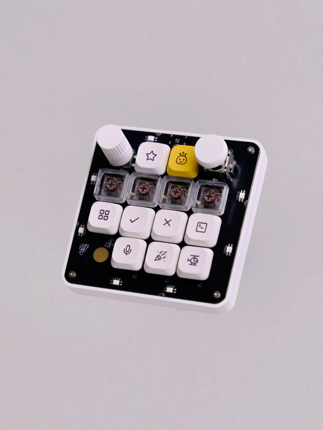
One standing rule for anyone who builds one: keep the SWD socket reachable. BOOT0 is held low on this board, which makes J2 the recovery path if power is lost during a firmware update.
If you change the board
The interesting case is not ordering this board — it is ordering a modified one. Change the CoHDL source in hw/v1/src/ and the BOM regenerates from the design; change the layout and the Gerbers and CPL regenerate from the board:
# from hw/v1/
cohdl build                       # -> out/openmicro-bom.csv

kicad-cli pcb export gerbers -o fab/gerbers/ \
  --layers F.Cu,In1.Cu,In2.Cu,B.Cu,F.Paste,B.Paste,F.Silkscreen,B.Silkscreen,F.Mask,B.Mask,Edge.Cuts \
  pcb/openmicro.kicad_pcb
kicad-cli pcb export drill -o fab/gerbers/ --excellon-separate-th pcb/openmicro.kicad_pcb

smt_pos.py pcb/openmicro.kicad_pcb out/openmicro-smt.csv
smt_pos.py lives in the open-source CoHDL repository. Re-zip fab/gerbers/ and you have a fresh order package.
The reason this is worth pointing out: the schematic is source code, so a change to the design is a diff you can read, review, and argue about — and the fab package that comes out the other side is regenerated rather than hand-maintained. That property is the whole point of the project.

Build one
Everything referenced above is in github.com/conol-ai/openmicrokbd:
- The order package —
hw/v1/fab/, with its own README covering fab parameters, the accepted DRC flags, and programming - The routed board —
hw/v1/pcb/openmicro.kicad_pcb, opens in KiCad 10+ - CoHDL schematic source and generated outputs —
hw/v1/src/,hw/v1/out/ - Printable case, knob, joystick cap, packaging and the soldering jig —
hw/v1/mechanical/, or ready to slice on MakerWorld (中国站) - Datasheets for every active, connector and electromechanical part —
hw/v1/docs/ - Firmware and companion app —
fw/,app/
Set it to 4 layers and ENIG, upload three files, check the placement preview. That is the whole secret.
If you order a set, or if something in the flow has changed since the video, say so in the Discord — fab interfaces move, and this guide should move with them. And if you modify the design before you order it, that is the outcome I was actually hoping for.